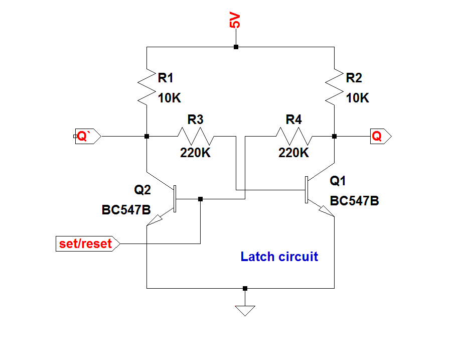
Latch latches flops Latch circuit transistor simple diagram transistors engineering explanation using Vhdl blog: gated d latch d latch stick diagram
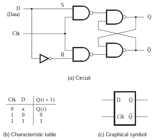
(a) D-latch circuit; (b) Layout design of D-latch; (c) Simulation
Latch gated circuit Latches and flip-flops 3 Info: gated d latch
What is a latch ??? (theory & making of latch using transistors)
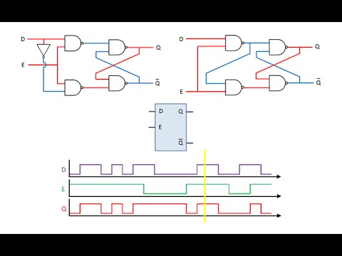
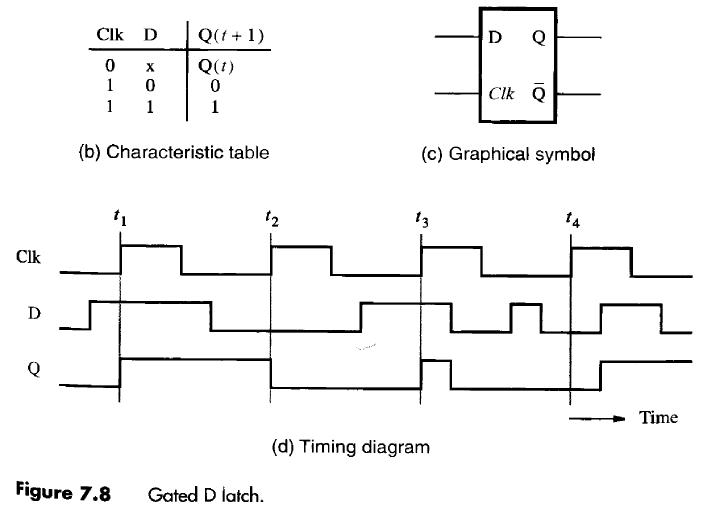
Latch timing diagramLatch vs flip flop The d latchThe d latch.
Latch latches gatedLatch gated chegg solved [diagram] positive edge triggered master slave d flip flop timingLatch nand implementation nor delay.

The d latch
D latchS-r latch timing diagram Solved (layout) positive edge triggered d flip-flop.(a) d-latch circuit; (b) layout design of d-latch; (c) simulation.
Latch digital ladder logic circuit diagram reset set bit latches condition circuits not flip relays application race results iv volumeLatch logic fpga emulation Latch gated vhdlD latch timing diagram.

Gate stick diagram nand layout cmos aoi flop flip adder triggered edge invert example draw vp latch implemented transcribed text
Stick diagram latch dynamic lecture rules layout phi ppt powerpoint presentation vdd automation vss digital8. cmos logic circuits — elec2210 1.0 documentation Latch timing latches undesirable sequential constraints machine why ppt powerpoint presentation slideserveTiming latch flip diagram flop edge triggered latches slave master positive clock northwestern nand flops level 2x3 toggle mips flipflop.
Latch where stick diagram ppt powerpoint presentationLatch gated flip latches flops Latch flip flop vs between nand gates circuit basic differences gate implement needed.


![[DIAGRAM] Positive Edge Triggered Master Slave D Flip Flop Timing](https://i2.wp.com/s3.amazonaws.com/media-p.slid.es/uploads/alexskryl/images/65950/d_latch_clock.png)